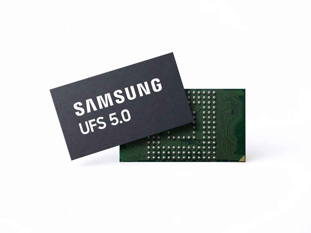
Samsung has built a new UFS 5.0 storage chip that the company says is the fastest in the industry and is designed to handle AI workloads directly on mobile devices. The chip is based on the latest embedded memory interface specification from JEDEC and supports a bandwidth of up to 10.8 gigabytes per second (GB/s).
Read speeds top out at 10.8 GB/s and write speeds at 9.5 GB/s, over double what the outgoing UFS 4.1 standard offers. According to Samsung, this translates into lower latency and quicker response times when large language models (LLMs) run locally on a device, rather than in the cloud.
Samsung also claims a power-efficiency gain of more than 40% over UFS 4.1. The improvement comes from clock gating and multi-voltage technologies that lower the power draw needed to move the same volume of data, which should help extend battery life on devices using the chip.
Physically, the new chip shrinks to 7.5mm x 13mm x 0.9mm, a 16.7% reduction from the previous generation. The smaller size gives device makers more room to work with in phones, wearables, and XR headsets.
Samsung plans to start mass production in Q4 2026, with capacities scaling up to 1TB. The company is positioning the chip for flagship smartphones, XR headsets, and AI wearables.


Leave a Reply